Closing the Voltage Loop With a PR Controller: Filter Resonance, Finite Gain and Non-Linear Loads
The question
A proportional-resonant (PR) controller is the textbook choice to regulate a sinusoidal voltage: it is supposed to deliver zero steady-state error at the fundamental. In this model, however, the output settles at 89 % of the reference, and under a rectifier load the waveform flattens at the top.
Neither effect is a numerical artifact. Both follow directly from the model parameters, and both can be predicted with a two-line calculation.
Model
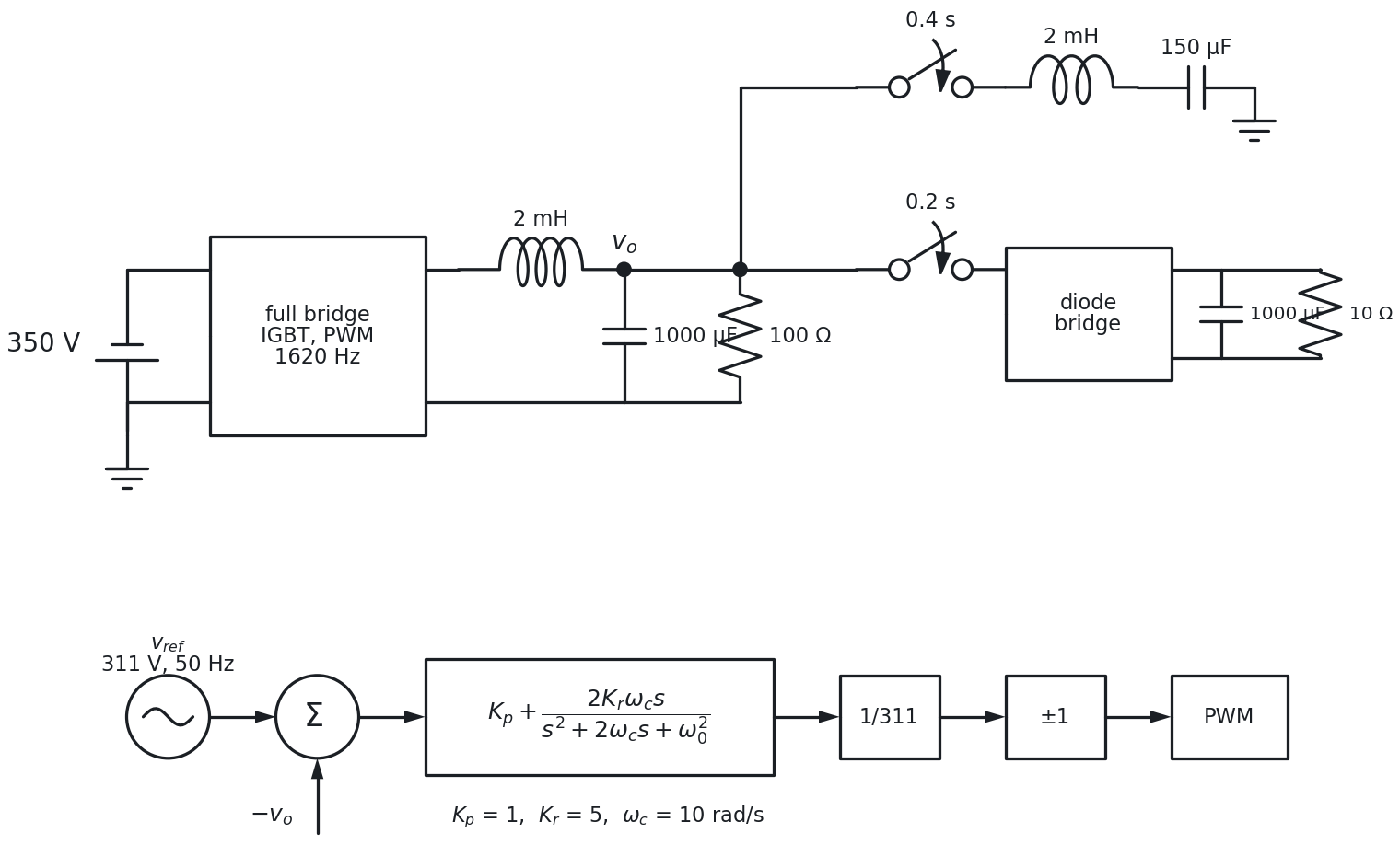
A single-phase full-bridge IGBT inverter, fed from an ideal DC link, drives an LC filter with a resistor across the capacitor (Figure 1). The output voltage is compared with a 50 Hz reference; the error goes through a PR controller, is normalized by 1/311, limited to ±1 and fed to the PWM generator. Two breakers connect a non-linear load (diode bridge with a capacitive DC stage) at 0.2 s and a linear series RLC load at 0.4 s.
| Element | Value |
|---|---|
| DC link | 350 V (ideal source) |
| Filter | L = 2 mH, C = 1000 µF, R = 100 Ω across C |
| Filter resonance | fr ≈ 112.5 Hz, Q ≈ 71 |
| Carrier frequency | 1620 Hz |
| Reference | 311 V peak, 50 Hz (220 V RMS) |
| PR controller | Kp = 1, Kr = 5, ωc = 10 rad/s, tuned at 50 Hz |
| Modulator limit | ±1 after normalization by 1/311 |
| Non-linear load (0.2 s) | diode bridge, 1000 µF, 10 Ω |
| Linear load (0.4 s) | series RLC: 2 mH, 150 µF |
| Simulation | discrete, 1 µs step |
The resonance frequency and quality factor of the filter are
f_r = \frac{1}{2\pi\sqrt{LC}} \approx 112.5\ \text{Hz}
Q = R\sqrt{\frac{C}{L}} \approx 71
The resonance sits only 2.25 times above the fundamental. That single fact explains most of what follows.
Results
Open loop: saturation plus resonance
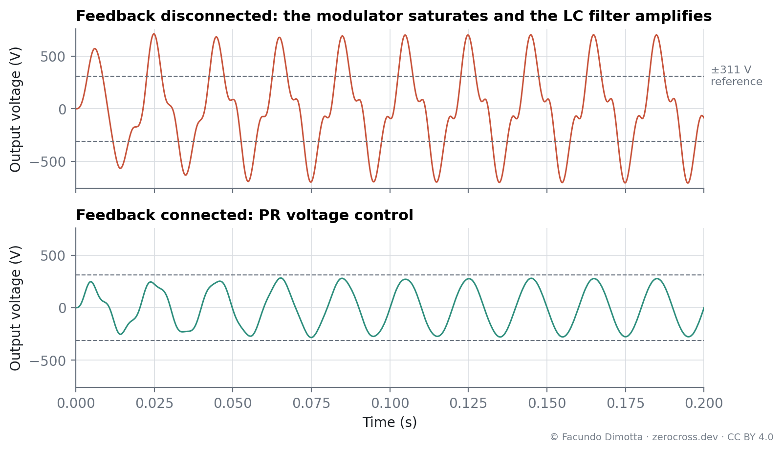
With the feedback disconnected, the reference goes straight through the controller. At 50 Hz the PR gain is Kp + Kr = 6, so the modulator is driven six times beyond its limit and the inverter produces an almost square voltage (Figure 2, top). Its fundamental is about \tfrac{4}{\pi}\cdot 350 \approx 446 V. Because 50 Hz is close to the filter resonance, the filter amplifies it by
|H(f_1)| \approx \frac{1}{1-(f_1/f_r)^2} = 1.25,
which predicts a fundamental of about 555 V. The simulation gives 575 V, with peaks of about 660 V and a THD of 20 %.
Closed loop: 89 % of the reference
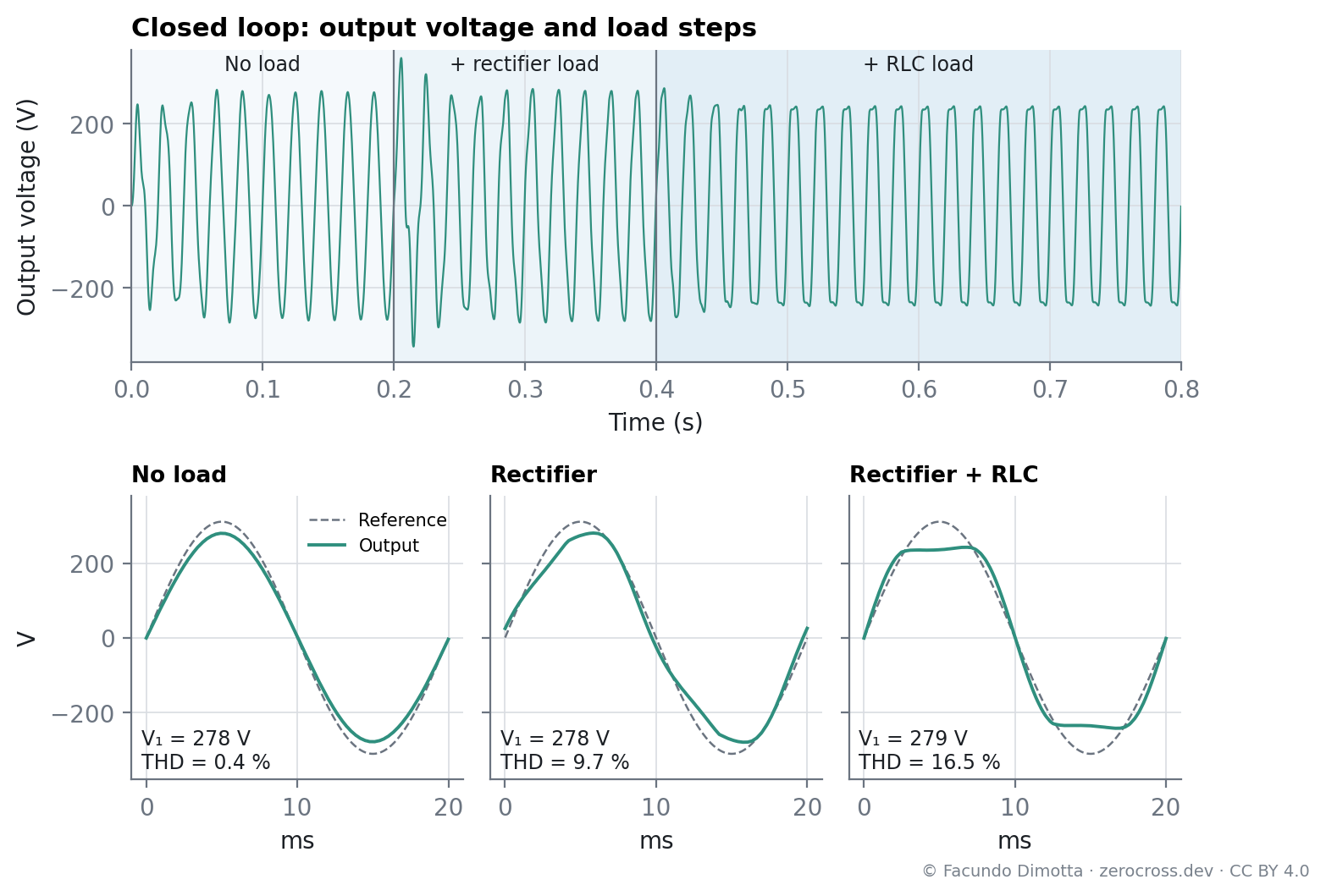
With the loop closed, the resonance is gone within four cycles and the waveform is clean (THD 0.4 %). But the fundamental settles at 278 V, not 311 V.
The cause is the non-ideal PR controller. The ideal PR has infinite gain at the fundamental; this one, with the damping term ωc, has a finite gain Kr = 5. The loop gain at 50 Hz is then
T(f_1) = V_{dc}\,|H(f_1)|\,\frac{K_p+K_r}{311} = 350 \cdot 1.25 \cdot \frac{6}{311} \approx 8.4
and the closed-loop gain at the fundamental is
\frac{V_1}{V_{ref}} = \frac{T}{1+T} \approx 0.894 ,
that is, 278 V. The simulation matches this value exactly. The modulator is not the limit: its input never exceeds 0.77, below the saturation limit of 1.
Load steps: flat-topping
The rectifier draws current only near the voltage peaks, and the controller, tuned only at 50 Hz, does not correct the resulting harmonics. The voltage flattens at the top (Figure 3): THD rises to 9.7 % with the rectifier, and to 16.5 % when the RLC load is added. The fundamental stays at 278–279 V throughout.
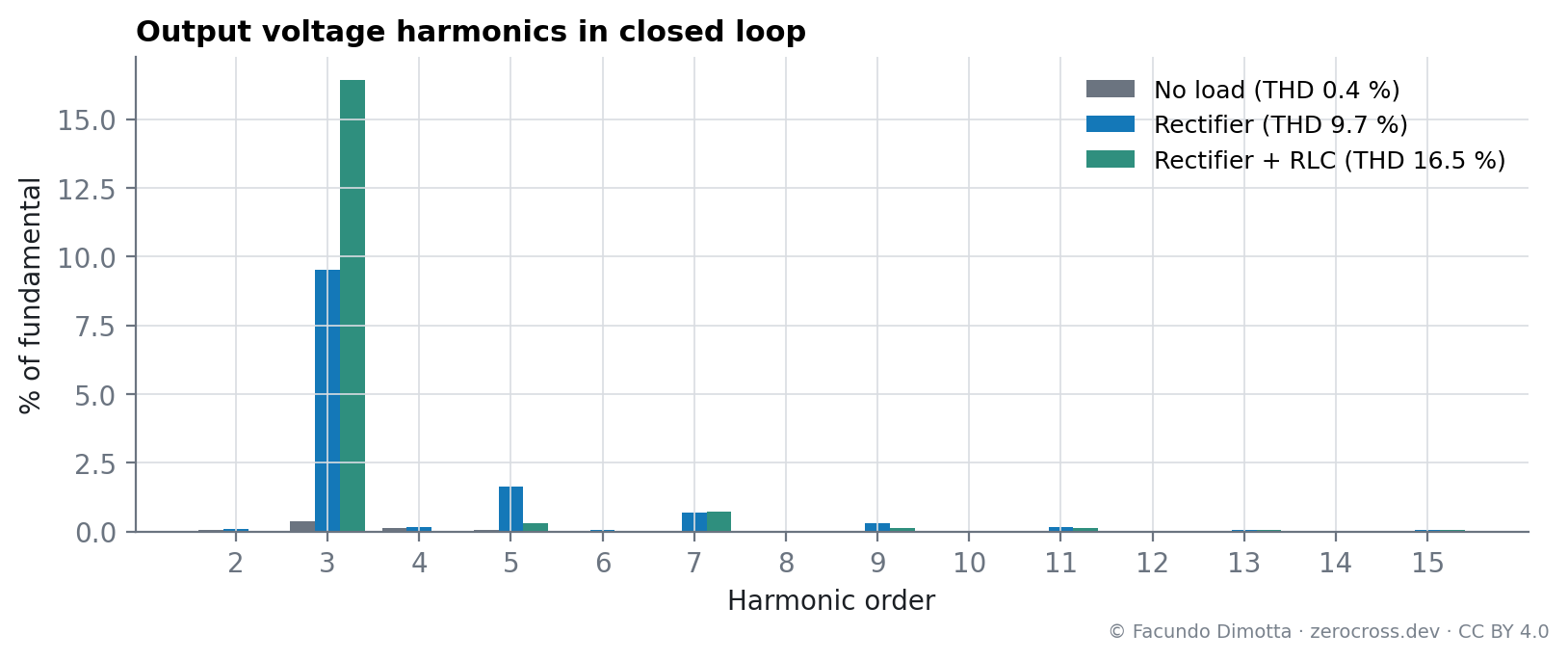
Almost all the distortion is third harmonic (Figure 4): about 9.5 % of the fundamental with the rectifier and about 16.4 % with both loads.
Does the loop reject the harmonics? No: it amplifies them
A fair way to answer this is to compare the closed loop with a true open loop: no feedback, no resonant term, and a fixed modulation index (0.638) that gives the same 278 V fundamental. With the rectifier connected, the open loop has a THD of 4.0 %; the closed loop, 9.7 %. The third harmonic grows from 3.8 % to 9.5 % of the fundamental (Figure 5).
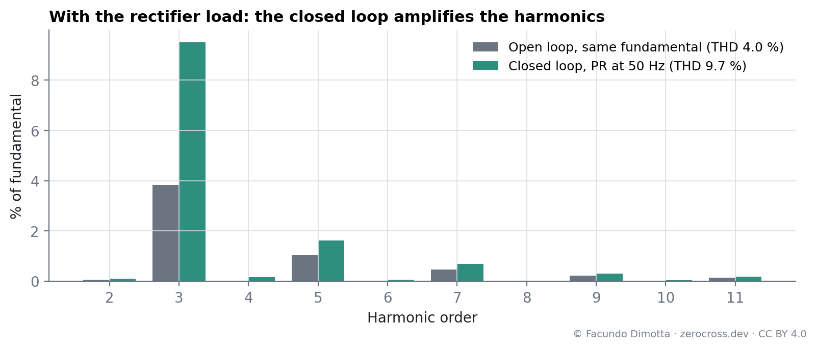
The loop gain explains why. Above the filter resonance (112.5 Hz), the LC filter inverts the phase of the signal. At the third harmonic the loop gain becomes negative, T(3f1) ≈ −1.46, so the proportional feedback turns into positive feedback. The sensitivity function, which tells how much the loop multiplies a disturbance, is greater than one at every characteristic harmonic:
| Harmonic | Loop gain T | |1/(1+T)| | Effect of the loop |
|---|---|---|---|
| 1st (50 Hz) | 8.41 | 0.11 | reduces the error to 11 % |
| 3rd (150 Hz) | −1.46 | 2.10 | amplifies about 2× |
| 5th (250 Hz) | −0.29 | 1.40 | amplifies |
| 7th (350 Hz) | −0.13 | 1.15 | amplifies slightly |
The simulation agrees: the third-harmonic voltage per ampere of third-harmonic load current is 2.3 times higher in closed loop than in open loop. In this design, then, the loop neither damps the harmonics nor compensates them. Note also that for a single-phase rectifier the dominant harmonic is the third, not the 5th and 7th typical of three-phase bridges.
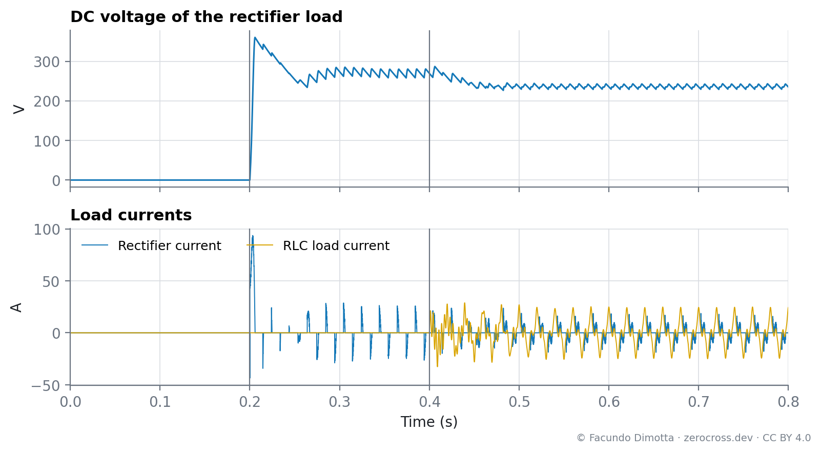
The DC voltage of the rectifier load follows the flattened peak (Figure 6): it jumps to about 360 V at connection, when the discharged capacitor charges through the filter, and settles at about 236 V with both loads.
Discussion
- Place the filter resonance well away from the fundamental. Here it sits at 2.25 × f1, where it amplifies the fundamental and any low-order harmonic, and falls inside the bandwidth the controller has to handle. A common design guideline places it roughly between 10 × f1 and half the switching frequency. With the same inductor, that means a much smaller capacitor.
- A non-ideal PR does not guarantee zero error. Its gain at the fundamental is finite and sets the steady-state error, as the calculation above shows. Raising Kr or reducing ωc brings the output closer to the reference, at the cost of stability margin and sensitivity to frequency deviations.
- Non-linear loads need harmonic control, and a filter that allows it. A PR tuned only at 50 Hz does not compensate the harmonics; with the resonance below the third harmonic, this loop amplifies them. The usual remedy is to add resonant terms at the 3rd, 5th and 7th harmonics, but those terms only work if the loop keeps enough phase margin at those frequencies, which again depends on where the filter resonance sits.
- This is voltage control, not active damping. The closed loop suppresses the open-loop oscillation, but active damping usually refers to specific techniques, such as capacitor-current feedback or a virtual resistor, that add damping to the LC resonance itself. That is a natural next step for this model.
Limitations
- The DC link is an ideal source; a real one would sag during the load steps.
- Switches are ideal and there is no dead time.
- The carrier frequency (27 × 60 Hz) and some powergui settings come from a 60 Hz template. They do not change the conclusions, but a revised model should use values chosen for a 50 Hz system.
2026-09-22. Rewritten after re-running the model and extracting its parameters:
- Figures regenerated from the simulation data instead of scope screenshots.
- The cause of the reduced amplitude was corrected. The original version attributed the ~240 V peak to the DC-link and modulation limits. An intermediate revision attributed it to controller saturation. Both were wrong: the controller output never exceeds 0.77. The 89 % amplitude comes from the finite gain of the non-ideal PR controller, and the ~240 V flat top from the non-linear load.
- Added the filter resonance (112.5 Hz), which the original did not report, and the calculations that reproduce the simulated values.
- Added the open-loop vs closed-loop harmonic comparison, following a question from readers on LinkedIn about whether the loop rejects the rectifier harmonics. It does not: in this design it amplifies them.
- The system had been called a solid-state transformer (SST); it is a single-phase inverter with an LC filter.
- “Active damping” was used for the PR voltage loop; clarified what the term usually means.
Reuse
Citation
@online{dimotta2026,
  author = {Dimotta, Facundo},
  title = {Closing the {Voltage} {Loop} {With} a {PR} {Controller:}
    {Filter} {Resonance,} {Finite} {Gain} and {Non-Linear} {Loads}},
  date = {2026-08-27},
  url = {https://zerocross.dev/posts/2026-08-27-pr-voltage-control-single-phase-inverter/},
  langid = {en}
}